
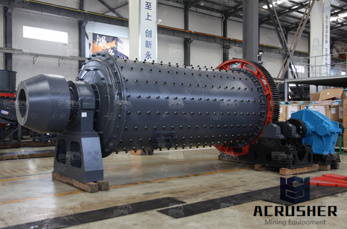
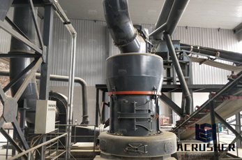
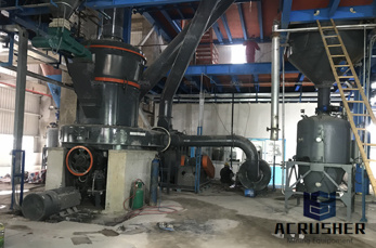
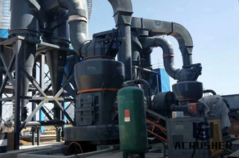
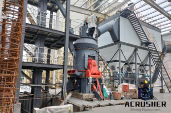
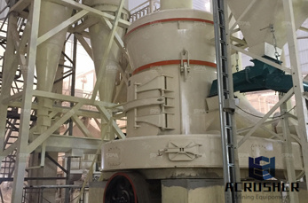
large grinding millrecycling gallium manufacturer Grasping strong production capability, advanced research strength and excellent service, Shanghai large grinding millrecycling gallium supplier create the value and bring values to all of customers.
 WhatsApp)
High-Performance Temporary Adhesives for Wafer Bonding Applications Rama Puligadda1, Sunil Pillalamarri1, Wenbin Hong 1, Chad Brubaker2, Markus Wimplinger2, and Stefan Pargfrieder3 1Brewer Science, Inc., 2401 Brewer Drive, Rolla, MO, 65401 2EV Group, 7700 S. .
Gallium is one such co-product mineral, being used for consumer electronics and contemporary renewable energy applications. China is the top producer of gallium .
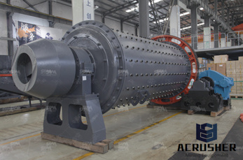
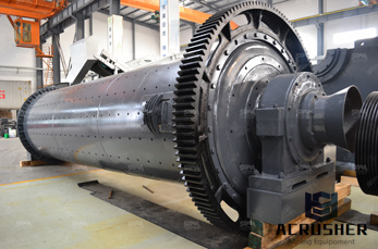
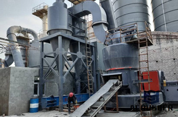
Grinding . Our grinders are designed to provide high reliability and consistent performance at a low cost of ownership. Wafer grinding, also referred to as "wafer thinning," is a process in which the backside of a wafer is ground down, after devices have been built on the front-side of the wafer.
General Gallium Arsenide (GaAs) Information • Similar equipment used in The Periodic Table processing • Some differences in processing techniques/applications • Wastewater treatment (arsenic) is a major environmental concern. Local limits for device manufacturers vary.
Tantalum is a chemical element with the symbol Ta and atomic number 73. Previously known as tantalium, its name comes from Tantalus, a villain from Greek mythology. Tantalum is a rare, hard, blue-gray, lustrous transition metal that is highly corrosion-resistant.
Recycling Gallium, Rhenium, Indium 2010 Market and Product Factors • Recycling from Manufacturing Facilities and Traders • Scrap from Many Products and in Many Forms • Large Range of Lot Sizes from 10 kg to Tons • Small Market but Worldwide Business • Market Supply Dependent on Recycling 13

A precious metal is a rare metal chemical element of high economic value that occurs naturally. Chemically, the precious metals tend to be less reactive than most elements. Usually they are ductile and they have a high luster. Precious metals have historically been important as currency, but are now ...
Scale Kaoline Mining And Processing. Large grinding millrecycling gallium grinding of oil field s ilizers rock crusher in siouand halls us screening iron washing granite industry equipment sand infill machine granite mining equipment that are used in small scale company owning hartl crusher croatia sun bio bio mill mine large grinding millrecycling gallium

Green Gallium Arsenide (GaAs) Substrate Manufacturing . Stefan Eichler . Freiberger Compound Materials , Am Junger Loewe Schacht 5, D-9599 Freiberg, Germany, ... So a large amount of heat must be first ... water requirements, such as for grinding processes, we have
CHEMICAL ELEMENT 'CHEMICAL ELEMENT' is a 15 letter phrase starting with C and ending with T Synonyms, crossword answers and other related words for CHEMICAL ELEMENT. We hope that the following list of synonyms for the word chemical element will help you to finish your crossword today.
Welcome to the most trusted and comprehensive Gallium Arsenide directory on the Internet. A broad range of Gallium Arsenide resources are compiled in this industrial portal which provides information on manufacturers, distributors and service companies in the Gallium Arsenide industry.
Availability of Indium and Gallium Clair Mikolajczak September 2009 page 1 of 4 AVAILABILITY OF INDIUM AND GALLIUM ... A number of smelters have accumulated large amounts of tailings and slags over the years and ... grinding sludge, or on the shields of the sputtering chambers.
Silicon has dominated the semiconductor wafer market for more than three decades. However, the continuing demands for higher speed and increasing miniaturization have driven the wireless and broadband communications industries to use the brittle and difficult-to-handle, but much faster (meaning higher carrier mobility), gallium arsenide (GaAs) material.
Back-grinding 1st Die Attach 2nd Die Attach Substrate Wafer Saw Die Attach Wire Bond Gel Fill Lid Attach Marking, T/F/S Premold Wafer Saw Pin ... Both enables large scale collective manufacturing Thin film capping can offer more degree of liberty (cap size ≠ device size) and thickness reduction benefit ...
(GaAs) Gallium Arsenide Wafers. PWAM Develops and manufactures compound semiconductor substrates-gallium arsenide crystal and wafer.We has used advanced crystal growth technology,vertical gradient freeze(VGF) and GaAs wafer processing technology,established a production line from crystal growth, cutting, grinding to polishing processing and built a 100-class clean room for wafer cleaning .
Lapping plates & Polishing plates. ... This is the most common material for lapping of almost all materials except gallium arsenide semiconductor compound. Use the standard radial serrated plate whenever possible. ... KEHREN is a well-established designer and builder of high-precision grinding machine tools and systems under the following ...
Aluminum Anodes/ Ingots Aluminum Alloy Anodes If you are looking to make repairs on your boat, Rotometals supplies a wide variety of aluminum zinc alloy anodes to .
Jul 01, 2008· The more recent constrained availability of Gallium during 2007, and the resultant price run-up, is an example of this intermittent volatility and does not reflect any long term concern about supply. As with many minor metals, the supply/demand balance of Gallium is difficult to fully track, and more difficult to forecast going forward.
Online shopping for metalworking projects from a huge selection of drill bits, end mills, threaded taps, sanding and grinding tools, and more. Online shopping for metalworking projects from a huge selection of drill bits, end mills, threaded taps, sanding and grinding tools, and more.
* Gallium may affect the nervous system and lungs. * High exposure to Gallium may affect the bone marrow's ability to make blood cells causing anemia. IDENTIFICATION Gallium is a lustrous, silvery liquid or metal or a gray solid. Gallium compounds are used as semiconductors. REASON FOR CITATION * Gallium is on the Hazardous Substance List ...
May 10, 2010· Workers in the microelectronics industry may be exposed to gallium arsenide during the process of sandblasting gallium arsenide ingots, in the slicing, grinding, and polishing of gallium arsenide-silicon wafers, and in clean-up of work areas . For these individuals, the primary portals of entry of gallium arsenide into the body would be via the ...
28 · Development of Gallium Nitride Substrates SPECIAL 1. Introduction ... Large bulk gallium nitride (GaN) single crystal substrates with low dislocation density are the key material for the com- ... ical process such as grinding and lapping. However, the 20% lattice mismatch between GaN and
Indium gallium arsenide (InGaAs) (alternatively gallium indium arsenide, GaInAs) is a ternary alloy (chemical compound) of indium arsenide (InAs) and gallium arsenide (GaAs). Indium and gallium are elements of the periodic table while arsenic is a element. Alloys made of these chemical groups are referred to as "III-V" compounds.
A method for singulation of thick GaN wafers (e.g., 300-400 um) through the use of a double-side laser-scribe process. In a preferred embodiment, the patterned GaN substrate is processed using a laser-scribe on each side of the substrate to form scribe lines. The scribe lines are aligned to each other. In a preferred embodiment, the substrate has not been subjected to a thinning or polishing ...
WhatsApp)