
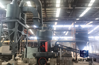
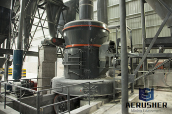
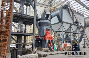
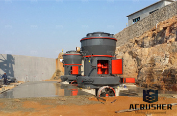
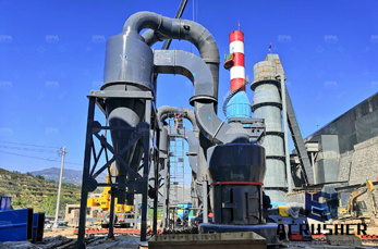
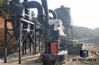
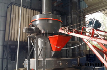
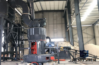
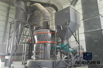
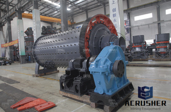
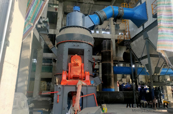
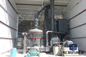
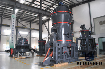
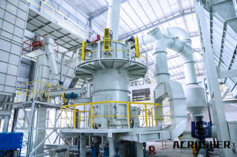
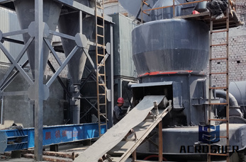
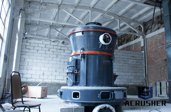
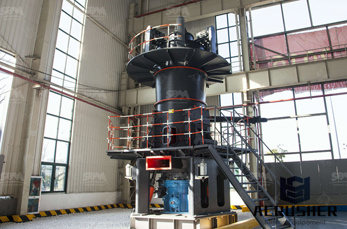
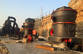
grinding process in mems manufacturer Grasping strong production capability, advanced research strength and excellent service, Shanghai grinding process in mems supplier create the value and bring values to all of customers.
 WhatsApp)
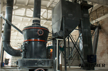
Technologies like RFID, MEMS Devices, and power devices are considered to be the major source of demand for these thin wafers. This scenario is increasingly creating demand for a better manufacturing process, especially processing and dicing which are important phases of ultra-thin wafer production. ... The grinding process in TAIKO leaves an ...
DEPRAG, Inc. End-of Arm-Tooling-Grinding & Polishing Automotive We are proud to introduce a new DEPRAG-Industrial product, the D-I End-of-Arm Grinding Module.This product was specifically developed for the automotive industry, but can also be used in any other. industry where there is a need for a stationary grinding- or polishing station. The Model No. is a MA 070-153V/S1.
polishing agent with added abrasive particles. Since then the process has seen a rapid evolution and was introduced into several areas of the IC production. The present work reports on studies to utilize CMP in the field of micro-electro-mechanical systems (MEMS) to create a new technology platform for
Why dicing-grinding service by DISCO? DISCO HI-TEC EUROPE's Dicing-Grinding Service (DGS) is an integral component of any manufacturing stage when it comes to high precision processing of ICs, MEMS, LEDs, other micro components and their inspection/metrology.
MEMS, MOEMS, sensors and other devices will be designed and fabricated with Stealth technology as the preferred medium for final singulation or dicing. The addition of Stealth Laser Dicing services fortifies our line of mechanical saws, which has been the de facto dicing standard for decades.
Many substrate materials can benefit from one or several grinding process to rapidly remove material, correct or optimize shape, and even achieve target surface finishes that can eliminate downstream processes. Grinding solutions for electronics are offered in partnership with Saint-Gobain Abrasives (Norton and Winter). Grinding Products
grinding process of MEMS based Micro grinding machine . are third level of spindle speed and second lev el of depth of . cut for achieving Larger material removal rate. V-CONCLUSION .
The Si-CMOS-MEMS process includes a grinding process followed by a bonding process and conventional post-CMOS etch. A Si-CMOS-MEMS accelerometer is used to demonstrate the feasibility of the Si-CMOS-MEMS process. A 0.2 µm flatness of ground silicon surface over 2 .
In the context of manufacturing integrated circuits, wafer dicing is the process by which die are separated from a wafer of semiconductor following the processing of the wafer. The dicing process can involve scribing and breaking, mechanical sawing (normally with a machine called a dicing saw) or laser cutting.All methods are typically automated to ensure precision and accuracy.
A SI-CMOS-MEMS process using back-side grinding - IEEE Xplore This paper presents a Si-CMOS-MEMS fabrication process which leaves the back-side silicon under the CMOS metal and oxide layers, and improves the ...
Grinding wheels may also be made from a solid steel or aluminium disc with particles bonded to the surface. Lubrication. The use of fluids in a grinding process is often necessary to cool and lubricate the wheel and workpiece as well as remove the chips produced in the grinding process.
Philips Innovation Services operates a state-of-the-art 2650 m 2 pure-play MEMS Foundry on the High Tech Campus in Eindhoven, the Netherlands. This MEMS Foundry is specialized in low to medium volume custom MEMS manufacturing.
The process frequency can act as an actuator on any part of the MEMS. Depending on the geometry and materials of the MEMS under consideration, it is necessary to analyze to likelihood of problems. If one of the eigenfrequencies of the MEMS or the WLTFP is (very) close to the bonding frequency, it may start to resonate.
are the influencing parameters of micro grinding process The micro grinding process of AISI 1020 has been optimized by Taguchi design noise ratio. L9 type of design is utilized to conduct II-APPLICATIONS MEMS based Micro grinder is very much useful for dental mechanic, micro valve lapping, micro cutting, tool grinding.
Mar 02, 2016· Back-grinding thin wafer de-bonding process, with UV dicing tape laminated.
The device for continuous gas density measurement in the process. Nanomass Gas Density is the first device for precise gas density measurement based on the revolutionary MEMS-Coriolis technology – a combination of innovative micro-technology and Endress+Hauser's long experience.
The process is purely physical and does not depend on parameters such as the temperature or wafer doping con-centration. Precision grinding of silicon proceeds in two stages: coarse grinding followed by fine grinding. During the coarse grinding stage, the wafer and grind wheel rotate at 200–250 rpm, the removal rate of silicon is about 250
Investigation of precision grinding process for production of silicon diaphragms A. Prochaska Abstract. The application of precision grinding for the formation of a S. J. N. Mitchell silicon diaphragm is investigated. ... coarse grinding followed by fine grinding. During ~MEMS! structures.

Revasum continues to invest in CMP and grinding technology targeted at the Semiconductor market for 200mm and below driven by rapid growth in the demand for nanotechnology for the IoT, power, RF communications, MEMS, LED, and other mobile applications, Revasum is leveraging Strasbaugh's core CMP and grinding technology to develop new ...
A SI-CMOS-MEMS process using back-side grinding. This paper presents a Si-CMOS-MEMS fabrication process which leaves the back-side silicon under the CMOS metal and oxide layers, and improves the uniformity of the back-side silicon using back-side grinding.
MEMS Dicing. Dicing takes a finished wafer (post-wafer fabrication) and converts it into individual dies; it's the step where the front-end fab process transitions to the back-end assembly process. Grinding & Dicing Services, Inc. has accumulated 25 years of engineering and process knowledge supporting semiconductor, consumer electronics, and ...
back-side silicon using back-side grinding. The Si-CMOS-MEMS process includes a grinding process followed by a bonding process and conventional post-CMOS etch. A Si-CMOS-MEMS accelerometer is used to demonstrate the feasibility of the Si-CMOS-MEMS process. A 0.2 µm flatness of ground silicon surface over 2 mm length is achieved in this work.
MEMS Bulk Fabrication Process Page 3 Rochester Institute of Technology Microelectronic Engineering DESIGN GUIDELINES Microelectromechanical Systems The basic unit of distance in a scalable set of design rules is called Lambda, l For the current MEMS process l is ten microns (10 µm) The process has eight mask layers, they are:

MEMS packaging accounts for 20-60% of the MEMS device BOM and is a key part of the MEMS function and design Packaging creates additional value as the MEMS device is integrated into a system (SiP, module) Standardization enables high volume production (second sourcing, cost efficiency through technology sharing)
WhatsApp)